1 Introduction
In surface mount applications, SMD adhesives are used to secure the SMD to the solder surface of the circuit board during wave soldering. In order to avoid component displacement under the influence of wave soldering, patch adhesives must be used. When the welding is completed, the patch glue no longer works.
The common component types that are bonded to the printed circuit board (Printed Circuit Board, PCB for short) solder surface are rectangular chip resistors and capacitors. The cylindrical transistor is a metal electrode face component (MELF) and Small outline transistor. These components are often wave soldered with a Through Hole Technology (THT) device.
2 Composition and Properties of Patch Adhesive
2.1 The chemical composition of the patch glue
Patch glue is usually composed of basic resin, curing agent and curing accelerator, toughening agent and inorganic filler, etc. The core part is the basic resin. At present, the basic resins commonly used are acrylates and epoxy resins, both of which have their own advantages and disadvantages, as shown in Table 1.
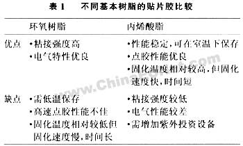
As can be seen from the above table, both have their own advantages and disadvantages, but due to the good electrical properties of epoxy resin and high bonding strength, most epoxy resins are currently used.
2.2 SMT adhesive packaging
SMT plastic packaging is generally divided into 20/30 mL syringe and 300 mL cartridge. The 20/30 mL syringe type is used for the spot coating process and the 300 mL cartridge type is used for the offset printing process.
2.3 Adhesive properties
There are many factors that must be taken into consideration when surface mounting an ideal patch adhesive. It is particularly important to keep in mind the following three main aspects: pre-cure characteristics, cure characteristics, and post-cure properties.
2.3.1 Characteristics before curing
For surface mounting, most epoxy adhesives are currently used. The currently used patch glues are colored, usually in red and orange. This is because the pad is coated with adhesive to affect the soldering, so this is not allowed. However, if the patch glue is of an easily distinguishable color, if it is used in excess so that it is applied to the pad, they are easily detected and removed. Uncured patch adhesives should have good initial tack strength. Initial tack strength refers to the strength of the patch glue before curing, that is, the components are temporarily fixed, thereby reducing flying or falling pieces when the components are mounted, and can withstand vibrations or bumps during mounting and transferring processes. Finally, the patch glue must be compatible with the sizing method used in production. At present, the sizing method of the circuit board uses a dot coating method, and the patch adhesive is required to adapt to various mounting processes, and it is easy to set the amount of sizing applied to each component, and the sizing amount must be stable.
2.3.2 Curing Characteristics
Curing properties are related to the curing time and curing temperature required to achieve the desired bond strength. The shorter the time to reach the desired bond strength, the lower the temperature, the better the patch glue. Surface mount patch adhesives must have a short curing temperature at low temperatures, and after curing they must have adequate bond strength to hold the components in place during wave soldering. If the bonding strength is too large, rework is difficult, whereas, if the bonding strength is too small, the components may fall into the solder bath. The curing temperature of the patch should be avoided to prevent board warpage and component damage. In other words, the patch adhesive is preferably cured at a temperature lower than the glass transition temperature of the circuit board (120°C for the FR-4 type substrate). However, a very short curing time above the glass transition temperature is generally acceptable. In order to ensure a sufficiently high productivity, a shorter curing time is required. Another feature of curing is that the amount of shrinkage during curing is small (minimizing the stress of the adhesive element).
2.3.3 Cured Properties
Although patch glue loses its effect after wave soldering, it affects component reliability in subsequent manufacturing processes such as cleaning and repair rework. One of the important characteristics of the adhesive after curing is that it can be repaired. In order to ensure the reworkability, the glass transition temperature of the cured adhesive should be quite low, and should generally be 75°C to 95°C. During the rework period, the temperature of the components often exceeds 100°C, because in order to melt tin-lead solder, the end connectors must reach much higher temperatures (>183°C). As long as the glass transition temperature of the cured patch glue is less than 100°C and the amount of the patch glue is not excessive, the reworkability is not a problem. The other importance of the adhesive after curing includes non-conductivity (under normal circumstances, the resistance of the glue surface is more than 8×10 11 Ω, it can be considered as qualified, that is, its insulation resistance is large enough, and the glue is open during normal operation. ), moisture resistance and non-corrosiveness. Patch adhesives should also have suitable insulating properties, but before final selection of patch glue, check the condition in the wet state.
3 SMT adhesive coating method and use process requirements
3.1 Application requirements of patch glue
3.1.1 Storage. Placing the adhesive on the conditions required by the supplier, its service life is calculated from the date of production of the package, and it is strictly prohibited to use it near the fire source.
3.1.2 Back to temperature. When epoxy adhesives are used, they are usually stored in a refrigerated environment at about 5°C in order to keep them as long as possible during storage. When you want to use it for production, you need to warm it up for a while. Normally, the temperature is returned at room temperature, and the temperature can not be less than 30 minutes. It is forbidden to use warming method to warm up.
3.2 glue coating method and process
3.2.1 glue coating method
There are many ways to apply glue. The commonly used methods are offset printing and dot coating:
(1) spot coating process. The so-called dot coating process is through the dispenser to apply the patch glue to the designated area of ​​the PCB (Figure 1). Pressure and time are important parameters for dot painting. They control the size and tailing of the dots. Trailing also varies with the viscosity of the adhesive, and changing the pressure can change the size of the dots. Hanging or trailing causes the “tail†of the patch to extend beyond the substrate surface of the component to the next area, and the patch glue covers the circuit board pad, which can cause poor soldering (Figure 2). Trailing can be reduced by making some adjustments to the dispensing system. For example: reducing the distance between the circuit board and the nozzle, using a larger diameter nozzle opening and a lower air pressure, will help reduce the hanging wire. If pressure is applied to the dispensing (this is a common case), any change in viscosity and limiting the flow rate will cause the pressure to drop, resulting in a decrease in the flow rate, which will change the dot size.
The viscosity of the patch glue also plays a role in forming the hanging thread. For example, stickies with larger viscosity are easier to hang than smaller stickies. However, if the viscosity is too low, the amount of glue may be too large. Since the viscosity changes with temperature, the change in ambient temperature may have a significant effect on the amount of glue. According to data reports: When the ambient temperature instrument changes 5 °C (15 °C to 20 °C), the amount of dispensing changes by almost 50% (from 0.13 to 0.19 g). All other dispensing variables, such as nozzle size, pressure, and time, have the same effect. In order to prevent the change of the glue point caused by the change of the ambient temperature, a constant temperature enclosure should be used. Leakage is another common problem in the application of patch glue. The possible cause of leakage is that the nozzle is blocked, the tip of the nozzle is worn, and the circuit board is uneven. If the glue is left unused for a long time (from hours to days, depending on the glue). The nozzle will usually be blocked. To avoid clogging the nozzle, clean it after each use and use a wire to connect the tip of the nozzle. In addition, a large viscosity may cause leakage of glue.
(2) Offset printing process. The so-called offset printing is through the screen printing process to offset the patch to the specified area of ​​the PCB, as shown in Figure 4, Figure 5. Although offset printing process and dispensing process have similarities, they belong to two different production processes. Compared with the latter, the offset printing process has such features as:
1 It can control the amount of printed rubber very stably.
For PCBs with pad pitches as small as 127 to 254 μm, the offset process can easily and stably control the thickness of the printed paste in the 50 μm ±0.2 μm range.
2 It can realize different sizes and different shapes of offset printing on the same PCB through one printing stroke.
The time needed to offset a PCB board is only related to the width of the PCB board and the speed of offset printing, and has nothing to do with the number of PCB pads. Dispensers place the glue on the PCB in order, little by little, and the time required for dispensing varies with the number of spots. The more glue points, the longer it takes to dispense.
Most customers who use offset printing technology are often very experienced in solder paste printing technology. The process parameters of the offset printing technology can be determined by using the process parameters of the solder paste printing technology as a reference point. Next we discuss how the printing process parameters affect the offset printing process.
1 stencil. Relative to solder paste printing, metal screens used for offset printing are relatively thick, typically about 0.2 to 1 mm. Considering that the glue does not have the property of self-converging to the PCB board pad during solder reflow, the size of the drain hole of the board should also be smaller, but it is better not to be smaller than the component pin size. Excessive amounts of glue will cause short circuits between component pins, especially when the shooter is difficult to achieve 100% perfect placement accuracy. For PCB boards with small pitch chips, special attention should be paid to chip pin short circuit.
2 printing gap / scraper. The print gap of the machine during offset printing is usually set to a small value (instead of zero) to ensure that the peel between the screen plate and the PCB plate occurs after the doctor blade printing process. If zero gap (contact) printing is used, a smaller separation speed (0.1 to 0.5 mm/s) should be used. Squeegee hardness is a relatively sensitive process parameter. It is recommended to use a harder scraper or metal scraper, because the low hardness scraper blade will "hollow out" the offset in the screen's leaky hole. With thin stencils, very high deposits can only be achieved when there is a certain print gap between the stencil and the PCB. The glue is pressed in the gap between the bottom surface of the template and the PCB during printing. Through the slow separation between the template and the PCB (eg, 0.5 mm/s), the glue is pulled out and falls, depending on the rheology of the glue, resulting in a more or less conical shape.
With contact printing, the dot height is limited due to the relatively small thickness of the template. The squeegee cuts off the glue with a large spot (for example, 1.8 mm) so that the height is almost the same as the thickness of the stencil. For medium-sized dots (eg, 0.8 mm), irregular dot shapes may occur because the adhesion to the template and the glue with the PCB is almost equal. During the separation of the template from the PCB, the template stretches the glue so that the glue dot height is greater than the template thickness. For the size of 0.3-0.6mm, part of the glue remains in the template because the adhesion of the adhesive to the template is better than that of the PCB. The height of these glue spots is low and the consistency is very good, as shown in Figure 5.
3 printing pressure / printing speed. The rheology of the glue is better than that of the solder paste. The offset speed can be relatively high, but it must not be so high that the glue cannot roll on the front edge of the blade. In general, the offset pressure is 9.8 to 98.1 kPa. Offset pressure should be just to scratch the surface of the stencil surface glue.
3.3 Factors Affecting Adhesion Effect
The sizing process should still be very important. It requires the material to be adhesive, like other adhesives, there are three factors that can affect the bonding effect: the amount of glue, SMD and PCB.
3.3.1 The amount of glue
The amount of glue required for bonding is determined by many factors, some users according to their own
Toy displays normally use plastic, injection plastic etc
Toy display stands,Toy Store Display Stand,Kids toy display shelving
Dongguan Display Leader Co., Ltd , https://www.displayonestop.com